Using the AD5627 DAC
DAC AD5627 level shifting
Introduction
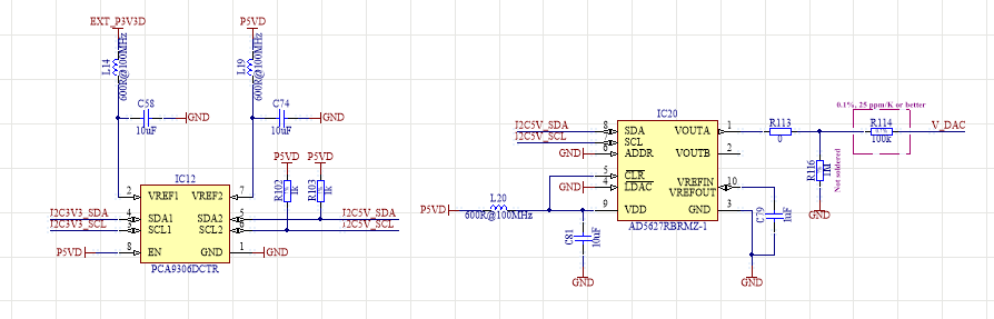
The AD5627RBRMZ (Datasheet) is part of a series of 12/14/16 bit nano DACs with an I2C interface. The DAC we are interested in is the 12 bit AD5627RBRMZ which has a 5ppm/˚C internal reference and can operate upto 5V.
Design
The DAC requires a high I2C level to be 0.8 * Vcc, which is 4V if we are interested in using the full capability of the DAC. In this design the I2C is operating on a 3.3 Volt bus, therefore, a bidirectional I2C level shiter is required.
For this I am using the PCA9306 Bidirectional I2C level shifter (Datasheet)
Circuit
Operation
Addressing
The 7 bit address is set by the fist 5 MSBs 00011 and the state of the ADDR pin.
| ADDR Pin Connection | A1 | A0 |
|---|---|---|
| VDD | 0 | 0 |
| No Connection | 1 | 0 |
| GND | 1 | 1 |
I have tied the pin to GND so the address is 0011 11 - 0xF
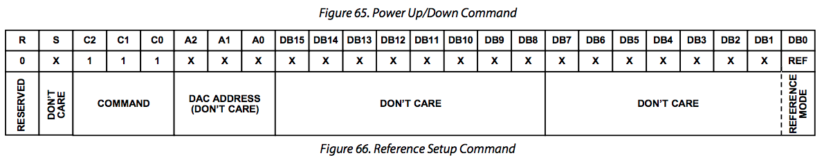
Set Internal Reference
On start up the internal reference is set to off. To turn it on send the command 0x38,0x00,0x01
Command - Internal reference setup (on/off) - 111
Address - Both DACS
Data - nothing
LDAC control - The DAC registers are updated after new data is read in.
Byte 1 - 0x3F - 00111111
Byte 2 - 0x00 - no data to send
Byte 3 - 0x01 - 0000001
Setting Output Voltage
The voltage is set with a 16 bit data string but as the DAC is 12 bits the last 4 LSBs are not used.
The voltage is set with a command followed by an address. command - Write to and update DAC channel n - 011 address - both DACs - 111
Bit 1 is reserved Bit 2 should be set to zero for 3 byte operation of chip
00011111 - 1F
Data - 12 bits to make full scale value FFF so 50% voltage would be 7FF.
last 4 bits should be set to 1 for operation - F
3 bytes = 0x1F,0x7F,0xFF
comments powered by Disqus